
Review on 🔧 Raytac MDBT42Q-DB-32 Nordic nRF52832 Module Evaluation Board Dev Kit Bluetooth ANT+ BT5.2 BT5 FCC IC CE Telec KC RCM SRRC Demo Board by Richard Mangum

Ideal BLE Development Board with NRF52832 Core Chip
It's easy to check because that's exactly what it says, it's nothing more than a simple development board based on NRF52832. It is 2 inches by 3 inches or approximately 55mm by 76mm. The board comes with a USB mini that you use to power the board. It says you can use it for coding and debugging, but I'm using JLINK, not USB Mini. The Jlink hookup wire also comes with a breadboard. No Jlink probe, just a wire. The headers are already soldered on, they are pin headers, not a hole. You can attach a female jumper directly to each pin. I use it with NRF 16 SDK. I'm a blind programmer so it's best not to give you a picture. I asked someone to describe the board to me so I know where everything is on it. This should help you decide if this board is right for you. The board is thin and flimsy, but I couldn't damage any of the three boards I bought. In other words, it's robust enough to be developed. Raytac Demo Board Description Looking at the board, the picture shows the chip on the left and the USB connector on the right. I'll describe it in columns because it seems natural to do it the way it's laid out. Jumper J12 is located directly above the chip. It has 16 pins. The top row of pins is labeled from left to right. , 22, 24, 20, 18, 16, 14, 12, 10 (yes, 22 and 24 are swapped as expected) The bottom row of cells is labeled left to right: 23, 21, 19, 17, 15, 13, 11 , 9 The designations refer to ports, ie P0.22, P0.24 etc. Then the IC goes under this jumper. Then under the chip is jumper J13. She has 16 contacts. Top row of pins labeled, left to right, 25, 27, 29, 31, 2, 4, 6, 8. Bottom row of pins labeled, left to right, 26, 28, 30, GND, 3, 5, 7, GDA J12, this is J14 NFC. It's not marked on the board itself, I found it on another drawing. It consists of 2 solder pads with through holes. The left hole is a round solder pad. The right hole is round with a square gasket. I believe it is for connecting an NFC antenna. Below the NFC jumper are solder pads for surface mount resistors and capacitors to complete the NFC circuit. Under the pads for soldering - SW4. This is a push button switch. connected to pin 4 of jumper J2. Below the switch are solder pads for two surface mount resistors. 1 for pull-up resistor to VCC. The other is for connection to P0.28, under SW4 and its resistance pad SW6 is a push button switch. This is for the pull up resistor to VCC. Under SW6 is jumper J11 (RS232). These are 2 rows of through hole solder pads, 4 in each row. 31, 30, 29, 28 are labeled on the right side, but in the schematic they are routed to contacts P0.06, P0.05, P0.04, P0.03. So, I'm not sure what's going on here. Bottom row, pins 1-4, all grounded. Also the RS232 port is on jumper J10, not J11. At the top, to the right of J14 NFC is jumper J9 (J-Link). These are 2 rows of through hole solder pads, 2 in each row. Top row, left to right, pins 1 2 are VCC and GND Bottom row, left to right, pins 3 4 are SWCLK and SWDIOB under J9 SW5 This is a push button switch. One end is grounded, the other end goes to pin 5 of jumper J2. To the right of the switch are solder pads for the SMD resistor. This is for the pull up resistor to VCC. Below SW5 is SW7. This is a push button switch. This is for the pull up resistor to VCC. Above, to the right of the pads for J9 (J-Link) is J1 (J-Link) These are 2 rows of pins Top row, left to right, pins 9 7 5 3 1, GND, unused, GND, GND, VCC Bottom row , left to right, pins 10 8 6 4 2, unused, unused, unused, SWCLK, SWDIO. I think this is where you could use the included ribbon cable to connect to your J-Link device. Below J1 (J-Link) - J6. This is a set of 2 solder pads. Left pad is pin 1, VCCI, right pad is pin 2 VCC. . It appears to be a 0 ohm resistor. To the top right of J1 (J-Link) are two large surface mount pads (I think) labeled BT. Contact pads are in a column. The top pad is marked with +. This is VCCI. The bottom pad is GND. Under the BT pads is the J7 jumper with some circuitry to the left of the jumper. The jumper consists of 2 pins aligned vertically. is GND. Immediately to the left of pin 1 and connected to pin 1 is the cap for GND. Under the cap is the XC6288D332VR chip. I can't find any information; I think it must be some kind of USB power controller? This is a 5 pin chip - 3 pins up, 2 down. Top row, pin 1 (VIN) and pin 3 (CE) are connected to 5V. Pin 2 (VSS) connected to GND Bottom row, pin 4 (NC) not connected. Pin 5 (VOUT) is connected to VCCI. There is another cap under the chip that goes between VCCI and GND. connected to VCCI on the left and to the green LED on the right. The other side of the LED is connected to pin 1 of J2. Additionally, on the right side of the LED are surface mount pads for adding a resistor that connects to P0.07Row 2 from left to right, the resistor connects to VCCI on the left. , and right is connected to the red LED. The other side of the LED is connected to pin 2 of J2. Additionally, on the right side of the LED are surface mount pads for adding a resistor that connects to P0.08Row 3 from left to right, the resistor connects to VCCI on the left. , and on the right are surface mount pads where you could add another LED. The other side of the LED goes to pin 3 of J2. No extra resistor, no extra connection to the main chip. Under circuit J6 and the LED, on the underside of the circuit board, is jumper J10. That's 2 rows. Each row has 3 through holes. must be RS232 and not the previously mentioned J11 jumper. Top row, left to right, pins 6, 5, 4 are GND, P0.19/CTS, P0.17/RX. They are bottom row, left to right, pins 1, 2 , 3 are VCC, P0.18/RTS, P0.21/TX. To the right of the BT pads is jumper J4 - this is a mini USB connector. ) connected to GNDPpin 1 (bottom) connected to 5V - so I think this chip must be some kind of USB power regulator? Below the mini-USB connector is jumper J2. A row of 7 plated through solder pads 1 (top) connect to the green LED. By adding a resistor it can also be connected to P0.07Pad 2 which is connected to the red LED. By adding a resistor it can also be connected to P0.08Pad 3 which is connected to the pads for the third LED. Pad 4 is connected to switch 4. It can also be connected to P0 by adding a resistor.28 Pad 5 is connected to switch 5. Pad 6 is connected to switch 6. Pad 7 is connected to switch 7.
- Computer Components
- Expensive
New products
Comments (0)
Top products in 🖥️. Single Board Computers
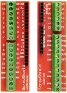
Gikfun Screw Shield Expansion Board: Enhance Arduino UNO R3 with the EK7007 Add-On

11 Review
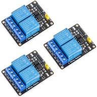
🌐 MCIGICM 2 Channel DC 5V Relay Module: Optocoupler Low Level Trigger Expansion Board for Arduino UNO R3, DSP, ARM, PIC, AVR, STM32, Raspberry Pi

11 Review
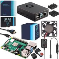
Vilros Raspberry Pi 4 4GB Complete Starter Kit - Black Fan-Cooled Aluminum Case for Heavy-Duty Performance

12 Review

55" TV LG OLED55C2RLA 2022 HDR, OLED, dark titanium

38 Review
Another interesting products
uxcell 3.5" HDD Screw Black 200pcs for Computer PC Case - Flat Phillips Head - 6#-32 - Hard Drive Fasteners

10 Review
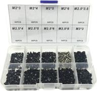
Comprehensive 500pcs Laptop Screw Kit Set for 🔩 IBM HP Dell Lenovo Samsung Sony Toshiba Gateway Acer

12 Review
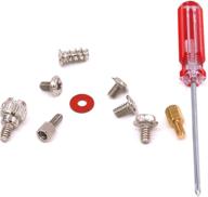
Glarks 660 Pieces Phillips Assortment Motherboard

10 Review
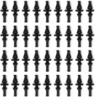
36-Pack Black Rubber PC CPU/Case Fan Screws/Rivets Set for Computer

11 Review

